Tags
Electronics production
- Eagle : Export PCBs quickly with this script
- Grow monitors | What watches the watchers?
- Networking light : Twin PCB
- Phototransistor breakout board
- EAGLE pt2 : Fabricating the circuit board
- Fabricating, wiring, learning
- LCD ATTiny44 PCB
- EAGLE pt1 : Designing a circuit board
- Stuffing a circuit board
- Milling a circuit board
Background
A printed circuit board (PCB) supports and connects electronic components via conductive tracks, pads, etc etched into copper which is laminated onto non-conductive substrate. PCBs can be single-sided, double-sided or even multi-layered. The electronic omponents (capacitors, resisters, processors, connectors, LEDs, etc) are soldered onto the copper zones of the PCB, a process known as stuffing. Once everything is properly connected, the microcontroller needs to be taught (programmed), which typically requires a programmer. This project involves three phases: milling the printed circuit board (PCB), stuffing the electronic components, and teaching the microcontroller to be a programmer.
Electronics production posts...
- Eagle : Export PCBs quickly with this script | 2018 Sep 24 | 2 minute read
- Grow monitors | What watches the watchers? | 2017 Jun 14 | 9 minute read
- Networking light : Twin PCB | 2017 May 16 | 3 minute read
- Phototransistor breakout board | 2017 May 01 | 1 minute read
- EAGLE pt2 : Fabricating the circuit board | 2017 Apr 07 | 3 minute read
- Fabricating, wiring, learning | 2017 Apr 06 | 2 minute read
- LCD ATTiny44 PCB | 2017 Apr 06 | 4 minute read
- EAGLE pt1 : Designing a circuit board | 2017 Feb 25 | 5 minute read
- Stuffing a circuit board | 2017 Feb 25 | 3 minute read
- Milling a circuit board | 2017 Feb 20 | 5 minute read
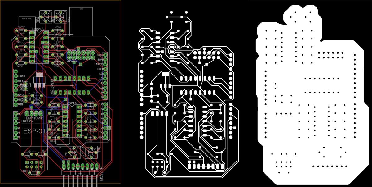
Exporting image files for milling PCBs is a tedious operation. Fortunately, Eagle has a built-in scripting interface. Customized scripts, spanning multitudes of operations, can be launched from the file menu. The following script, based on this one, will output two PNGs, one for traces and the other for the outline and holes. The PNGs can then be coverted to milling tool paths via Fab Modules. DISPLAY ALL; RATSNEST; DISPLAY None; DISPLAY Top Pads Vias; SET DISPLAY_MODE NODRILL; SET PAD_NAMES OFF; SET PALETTE BLACK; EXPORT IMAGE /*/pcb_traces.png MONOCHROME 1500; DISPLAY None; SET DISPLAY_MODE REAL; DISPLAY Pads; EXPORT IMAGE /*/pcb_outline.png MONOCHROME 1500;...
Simultaneous to the module development, I will produce some grow module monitoring equipment. Previously, I worked with a phototransistor sensor, an LCD output and wrote a basic graphical interface for live monitoring the phototransistor readings. Today, my goal is to combine these with voltage sensoring so I can begin tracking the correlation between sunlight and power generation in the bioelectrochemical testing modules. Starting with a little research, I found that by simply connecting an input voltage to an open ADC pin, I could take voltage readings. Duh. I have been doing this for weeks via the phototransistor. I returned to...
I was introduced to a project by Enrico Bassi which uses two ATMega boards connected to IR Sensors and IR LEDs to network by reading pauses in IR light (low). Upon seeing it, I was immediately impressed with the visceral qualities of networking with light. It is visible to our eyes! And, we could control a light in our hands to communicate to a machine. Admittedly, low tech stuff here. Remote controls... Plus, technically, we cannot see the light, the red LED on Bassi's board is for human reference, the IR LED is invisible to us. Regardless, as a first...
In a previous project based on an ATtiny44 I added an expansion pin on PA2 (ADC2/AIN1/PCINT2). I think I can use that pin to take readings from a phototransistor; making this a nice little project to get generate some momentum. Remember: spiral development. First I examined Neil Gershenfeld's ATtiny45 schematic, the ATtiny45 datasheet, the ATtiny44 datasheet, andthe OP580DA phototransistor datasheet. Because both pins are compatible with Analog to Digital Conversion (ADC), the phototransistor should work with my ATtiny44 board. The first step is to design a board for the phototransistor, resistor, voltage, ground, and logic connections. I use Autodesk's Eagle....
I need to export the board design from EAGLE, generate the mill paths and solder the electronic components. The board is ready to be cut; EAGLE's job is complete. Time to export. From the View> Layer settings... menu, set all the layers to invisible except Top, Pads and Dimension. Export the file as a monochrome PNG at 1500 dpi. The PNG may not be exported in perfect condition but can quickly be edited in a PNG suitable editor, i.e. Photoshop, Inkscape. I did not find a good way to export a PNG for the outline cuts. EAGLE has a thin...
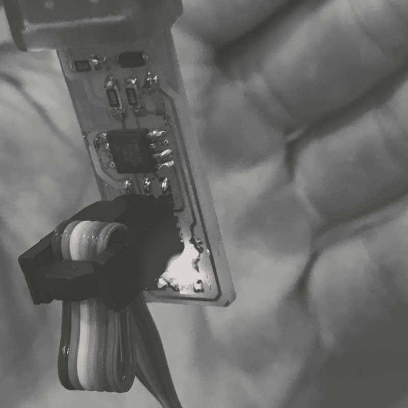
This dance is as follows: mill, solder, wire. Familiar aesthetic for the board. Milling the traces at 0.10mm depth once again was unsuccessful so I dropped the depth to 0.15mm and milled on top of the previously milled stock. Soldering was significantly faster. This time, when heating the connections I kept a count in my head which varied from an one to three count according to the size of the components. Worked well in terms of pace. Checked all the connections with a multimeter. No problems. Initially I connected an incorrect resistor in front of the LED which took me...
I am using a Lumex 16*2 character LCD Module. This LCD only requires 5v and six data pins to get up and running. I do not have a PCB with the free pins or proper configuration to use with this LCD. Not a problem however, because I have learned my way around designing, milling and stuffing PCBs. Get it. I started by inspecting Neil Gershenfeld's example LCD board. I posted a low resolution copy of the image here for convenient reference. The linked version is better. While following this is great for a beginner like me, I quickly became aware...
EAGLE is a scriptable printed circuit board (PCB) computer aided design (CAD) program for 1. creating relationships between electronic components, for which you may download and curate libraries, then 2. positioning the components on a PCB and drawing traces. EAGLE stands for Easily Applicable Graphical Layout Editor. As of 2016, EAGLE was acquired by Autodesk Inc. The EAGLE is split into two primary GUIs: Schematic and Board graphs. You will use the schematic graph to select and interrelate the electronic components to be soldered on the PCB. The board graph is used to arrange the components and draw traces, pads,...
Freshly produced PCB in hand, it is now time to solder the electronic components. Soldering is tricky. Repetition is key. I am beginning to find an effective method varying my practice, trial and error. This is a road map of component placement from the FabTinyISP page. First, gather the components, or do not. I soldered two boards. The first, I gathered everything beforehand, the second time I grab componenets from their storage as I went along. Whatever, both worked. Just be careful not to lose any or return to the wrongly marked storage. The microcontroller and diode components are directional;...
The PCB is composed of a thin layer of copper, measuring in just microns of thickness, laminated onto FR1, phenolic paper. The pattern of copper connects a series of electronic components with electricity. If any unintentional connections are made, the whole system may be fried. While in subsequent posts, I will explore designing the etching patterns, this time around, I am using an open-source project developed in the FabLab ecosystem: the FabTinyISP version of an AVR ISP programmer/board. You can download the same PNG files I used for the traces and the board outline and read detailed build instruction on...