Tags
Electronics production
- Eagle : Export PCBs quickly with this script
- Grow monitors | What watches the watchers?
- Networking light : Twin PCB
- Phototransistor breakout board
- EAGLE pt2 : Fabricating the circuit board
- Fabricating, wiring, learning
- LCD ATTiny44 PCB
- EAGLE pt1 : Designing a circuit board
- Stuffing a circuit board
- Milling a circuit board
2017 Feb 25
#electronics
#elecFab
EAGLE is a scriptable printed circuit board (PCB) computer aided design (CAD) program for 1. creating relationships between electronic components, for which you may download and curate libraries, then 2. positioning the components on a PCB and drawing traces. EAGLE stands for Easily Applicable Graphical Layout Editor. As of 2016, EAGLE was acquired by Autodesk Inc.
The EAGLE is split into two primary GUIs: Schematic and Board graphs. You will use the schematic graph to select and interrelate the electronic components to be soldered on the PCB. The board graph is used to arrange the components and draw traces, pads, holes, etc. Both interfaces present a working area flanked by buttons along the left and top. The mouse pans and zooms. Most of the buttons are self-explanatory making this a fairly easy application to initially grasp.
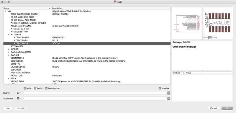
Start by importing electronic components from the libraries into the schematic graph. Click on the white plus sign just under the wrench button on the middle left. EAGLE comes preloaded with several libraries and users can make custom libraries. The FAB Academy has a custom library with all the electronic components commonly found within Fab labs. Very helpful. This board requires the following components:
- IC1 : 1x ATtiny44
- RES1, RES3 : 2x 10kΩ resistor
- RES3 : 1x 500Ω resistors
- LED : 1x red LED (directional)
- XTAL : 1x Panasonic ceramic resonator
- S1 : 1x OMRON switch
- CAP1 : 1x 1UF capacitor
- PIN : 1x 1x1 pin header (hole)
- ISP : 1x 2x3 pin header
- FTDI : 1x FTDI SMD header
Source the components in the library and press OK. Then, mouse click somewhere in the schematic graph to add one component. If multiple of the same, you can click twice or more. Or, you can copy later. Also, components can be moved around the schematic window any time throughout the design process.
One ATtiny44 placed in the schematic graph. All the connection points are numbered and labeled. Perhaps the functionality of some are more obvious than others. VCC is voltage in. GND is ground.
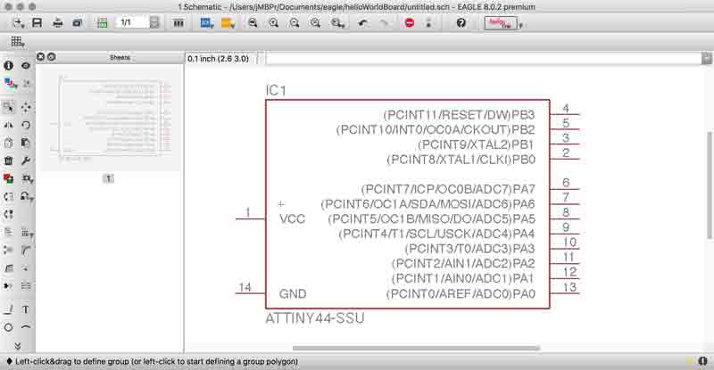
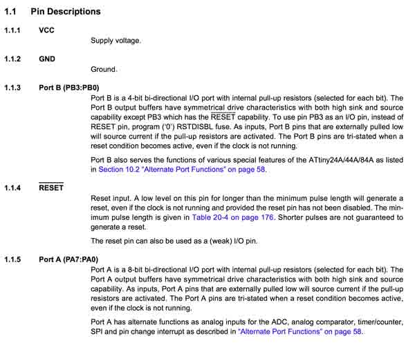
What about the others? Datasheets are your number one ally. Good news, the ATtiny44 datasheet has 286 pages of useful information, including pin descriptions!

After placing electronic components in the schematic window, connections need to be labeled. This can be done in two ways. One, using the pencil tool next to the "T", draw a line directly from one pin to another. Two, use labels, four buttons below the "T". Any labels with precisely the same name will be connected (although it is otherwise invisible).
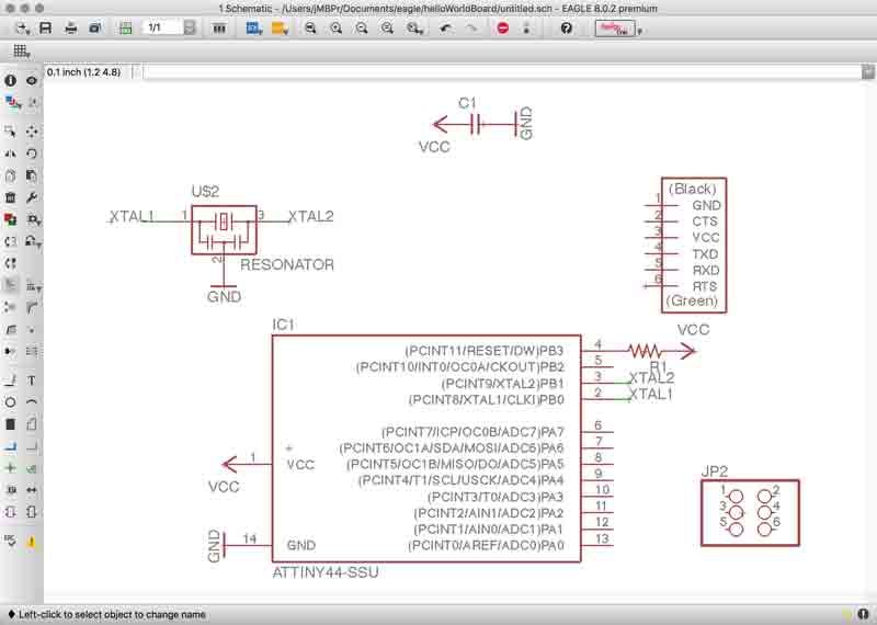
As connections are made, it is helpful to move the components around to double check that the connections were made. Sometimes things that appear connected are not and that could cause trouble later if not caught. For instance, you may cut a board with missing traces.
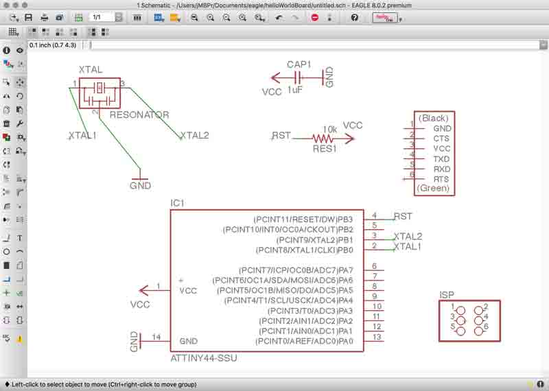
The schematic graph can be organized in any way, as long as the proper connections are drawn and/or labeled. I tried to present the arrangement with some clarity. Now that all components are connected, it is time to move into the board graph interface. Click the Generate/Switch board button on the top just to the left of the 1/1 pulldown.
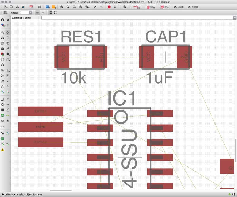
Now all the components will be displayed to scale with their connections to one another drawn with yellow lines. At first the components are piled up to the side. The basic interface is the same as the schematic window. Move the components into the general arrangement planned. Keep an eye on the yellow lines with an idea of how the traces may be aranged. Because this is a one sided board, traces cannot overlap. It is like drawing a maze, and it is challenging. I will return to this later in this section.
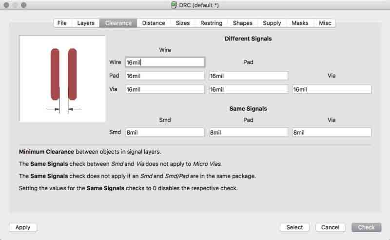
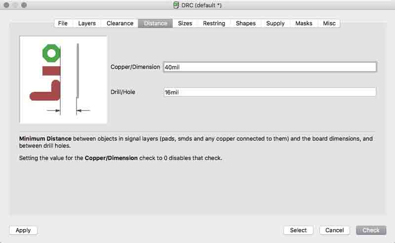
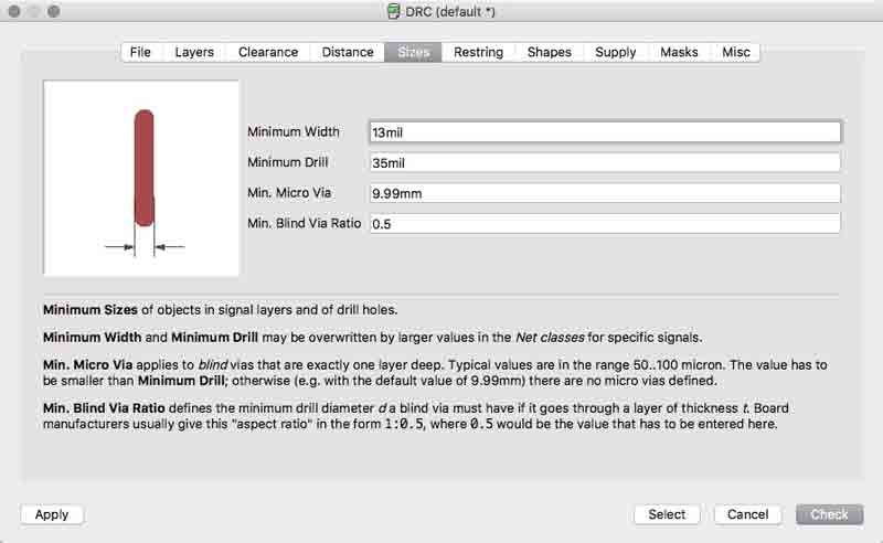
Setup design rules in accordance to the tolerances of your CNC mill or Vinyl cutter.
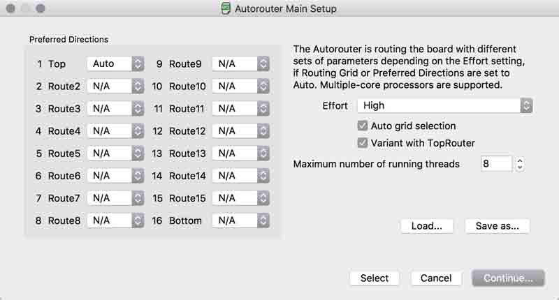
After the components are organized, EAGLE has an Autorouter feature. The application will try to draw the traces and pads to your design rules within your organization of electronic components. This PCB will be a single sided/layer design. Top: Auto. Bottom: n/a. Effort and threads are related to the amount of computing power you want to give EAGLE to solve this puzzle. Press continue and on the next dialogue, Start.
Autorouter will draw several variants to varying degrees of success. In this first test, the best result was missing connetions. Either accept this result and try to solve the problem yourself, or rearrange the electronic components and try the autorouter again. Opting for the latter, I did this process several times and by doing that, I learned about organizing the components.
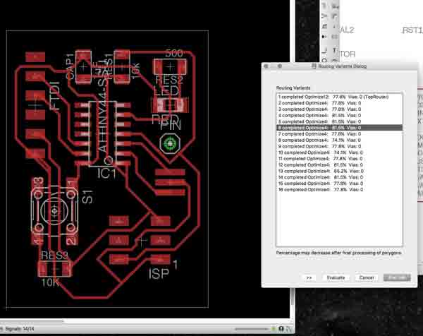
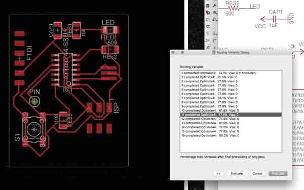
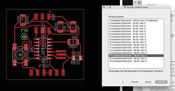
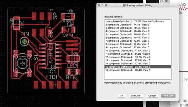

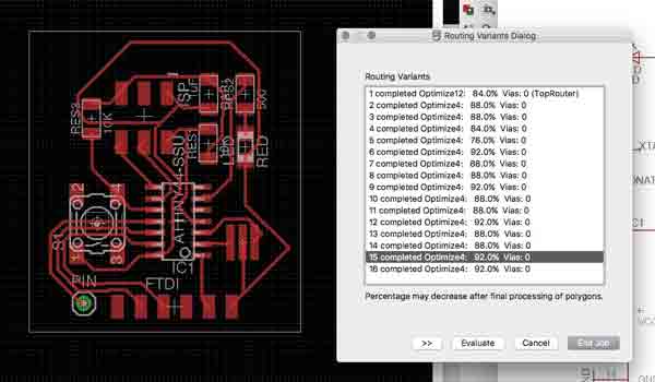
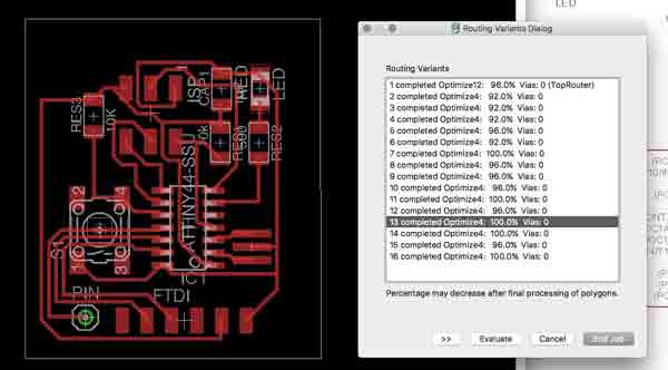
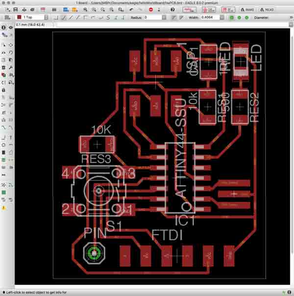
Fast forward a couple hours and I have a few 100% variants. Using this, I started adjusting the traces manually. There are two main tools for this process: Route and Ripup. The buttons are side by side in the row just above the "T". I was challenging myself to find a very compact arrangement. Unfortunately, the traces do not update as components are moved, so this process can become tedious in EAGLE.
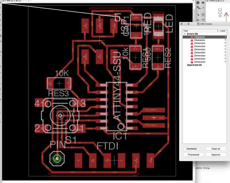
After the traces are settled, return to the design rule check (DRC) dialogue and run a check. This will show you conflicts with your rules. Make the necessary adjustments to resolve the errors.
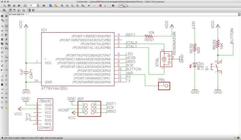
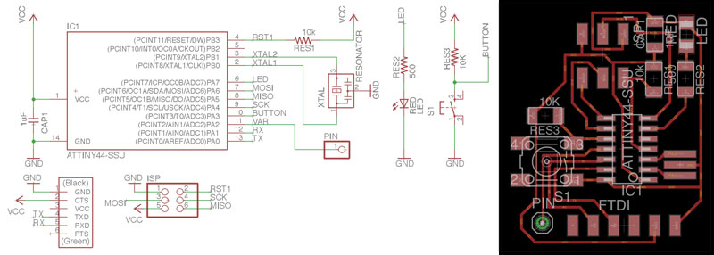
With that, my first PCB drawn from scratch. Here are the final schematic and board layouts.
Download project files
I will post links to resources I have found helpful here.
Share this post...
« Previous post :: Stuffing a circuit board
Freshly produced PCB in hand, it is now time to solder the electronic components. Soldering is tricky. Repetition is key. I am beginning to find an effective method varying my practice, trial and error. This is a road map of component placement from the FabTinyISP page. First, gather the components, or do not. I soldered two boards. The first, I gathered everything beforehand, the second time I grab componenets from their storage as I went along. Whatever, both worked. Just be careful not to lose any or return to the wrongly marked storage. The microcontroller and diode components are directional;...
Next post :: Three dimensional scanning wildCardboard »
I tried to scan one of my previous projects, wildCardboard with the Microsoft Kinnect using the Skanect application. How about starting with an image of the outcome? Plug the Kinnect into your computer's USB port then launch the Skanect application. The interface is straightforward. The first tab are variables for the type and size of the 3D scan. This model fits within an 300mmx300mmx300mm virtual bounding box. I will touch on this more later, I found it to work a little better to give plenty of extra space so in subsequent scans I added padding to the size of the...