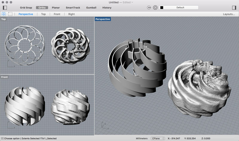
I tried to scan one of my previous projects, wildCardboard with the Microsoft Kinnect using the Skanect application. How about starting with an image of the outcome?
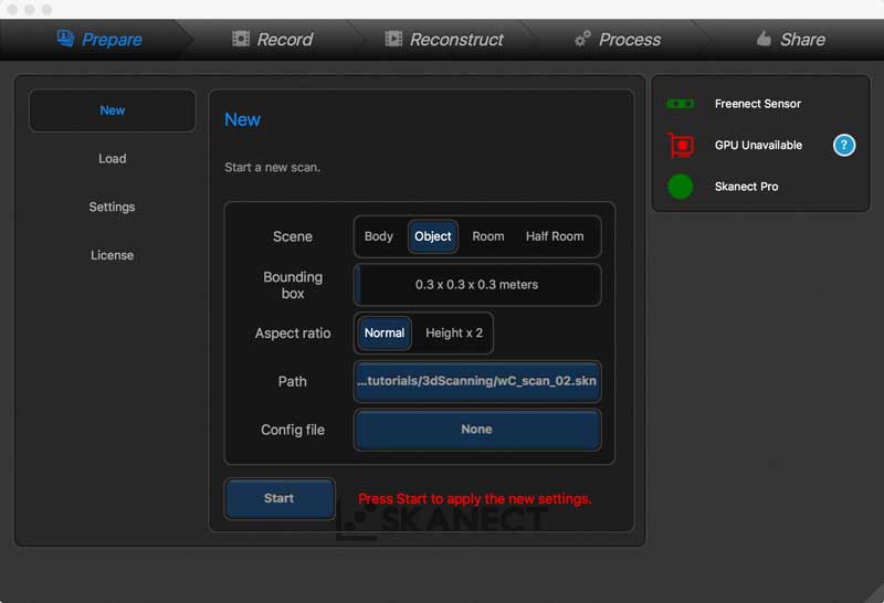
Plug the Kinnect into your computer's USB port then launch the Skanect application. The interface is straightforward. The first tab are variables for the type and size of the 3D scan. This model fits within an 300mmx300mmx300mm virtual bounding box. I will touch on this more later, I found it to work a little better to give plenty of extra space so in subsequent scans I added padding to the size of the bounding box, nearly double the size. As you will read, unwanted parts of the model can be removed later without the help of advanced 3D modeling applications.
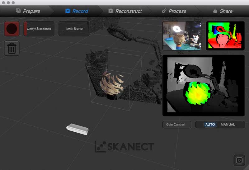
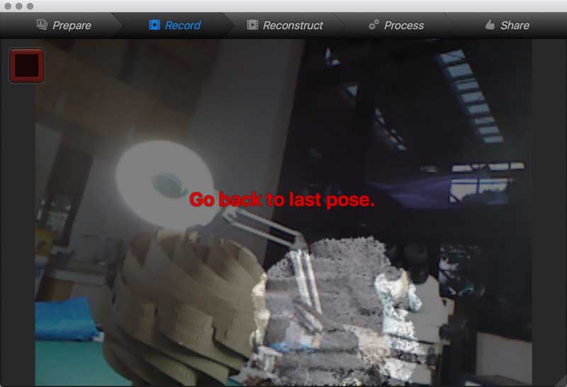
The next tab: Record, is where the important user action takes place. The Kinnect needs to be about 1.5m from the object. The interface helps to locate the scanner in relation to the object while the colorized largest window to the right gives color feedback from green to yellow to red. Green is a good distance for the scanner while red is too close or too far. Once in position, press the record button in the upper left corner.
I started by mounting the kinnect to a tripod and using a rotating plate with the cardboard model. Skanect was unable to work using this method. I thought perhaps it had to do with the repetitive nature of the cardboard model confusing the software. However, when trying a different objects, Skanect was just as stubborn in its refusal to produce. Skanect recommends using the Kinnect in hand and moving it around the model, so I moved to this method next.
Now utilizing the kinnect as a handheld scanner, you need to be careful about moving too quickly, getting too close or far from the model, or losing site of the model by obscuring a sensor or misdirecting the kinnect. Keep your computer model in your sightline and be mindful. If any problems happen, you may lose the model and either need to help Skanect find it or start over. I found as long as I was moving slowly, even if Skanect lost the model it was easy to replace becasue I had not strayed far. When I moved too fast, it would be a big problem.
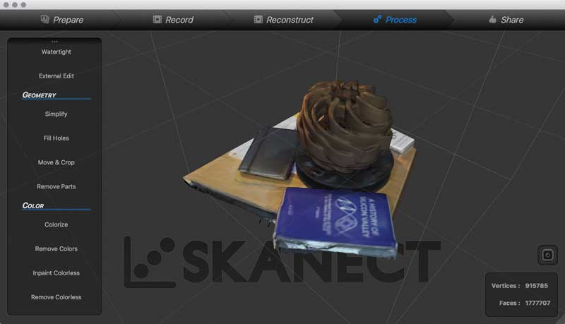
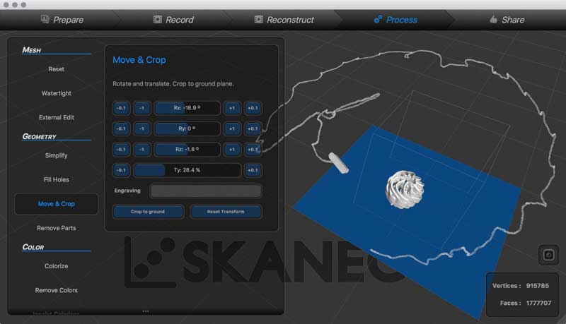
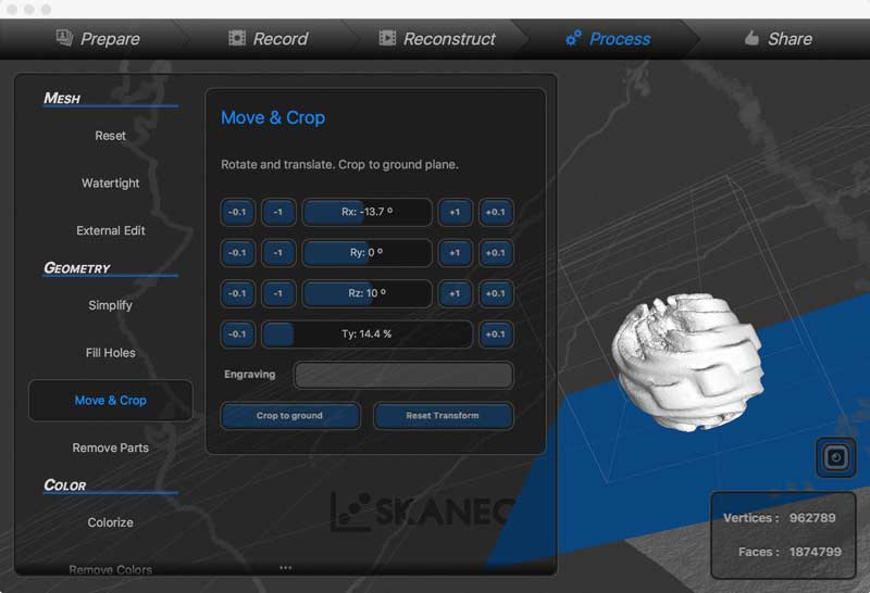
After recording, Skannect will quickly build a 3D model. Included in the process tab are simple interfaces for cropping undesired mesh, rotating, and adding texture maps. In the first image, I checked the texture maps. The second, I fixed the model alignment and cropped the books and table by moving the blue plane between those things and the model, then "crop to ground". This was my first successful scan. I can see the thicknesses of the material and the resolution between the ribbons has many mistakes. I resolved to try more scans varying my speed, increasing the surface area of my scanning, and adding more lights.
Two more scans and my results were essentially the same. I was able to get more detail inside the void and along the top and bottom but the wall thickness issues remain.
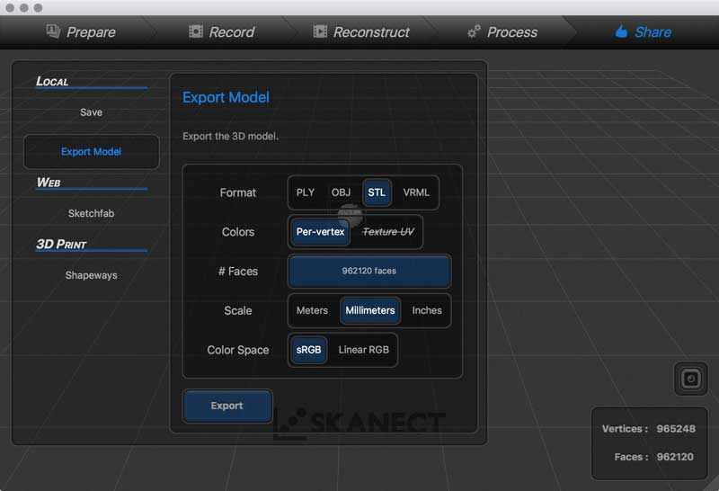
Finally, I exported the mesh as an STL file for use in other applications.
Here, you can see a comparison of the source CAD model and the scanned model. I think Skannect would work better with solid objects but I have trouble thinking of it as a tool for more than rough scans. Of note, the scale of the model was remarkably close to wildCardboard.
I will post links to resources I have found helpful here.
Share this post...
« Previous post :: EAGLE pt1 : Designing a circuit board
EAGLE is a scriptable printed circuit board (PCB) computer aided design (CAD) program for 1. creating relationships between electronic components, for which you may download and curate libraries, then 2. positioning the components on a PCB and drawing traces. EAGLE stands for Easily Applicable Graphical Layout Editor. As of 2016, EAGLE was acquired by Autodesk Inc. The EAGLE is split into two primary GUIs: Schematic and Board graphs. You will use the schematic graph to select and interrelate the electronic components to be soldered on the PCB. The board graph is used to arrange the components and draw traces, pads,...
Next post :: Mathematica model..? (no) »
I am forever in awe of math derived computer geometries. I would love to learn how to write scripts that generate models in a CAD application soon. For the first draft, I decided it would be much faster to sketch a model based on visual cues and test it in a 3D printer. I used Autodesk Maya for this sketch. This little thing fits within a 35mm radius sphere. I am trying to push the tolerances of machine to an extreme here. The first pass I will try 1.2mm wall thickness with some temporary scaffolding. I am forever in awe...