Tags
#electronics
#cut2d
#elecFab
#tutorials
Electronics production
- Eagle : Export PCBs quickly with this script
- Grow monitors | What watches the watchers?
- Networking light : Twin PCB
- Phototransistor breakout board
- EAGLE pt2 : Fabricating the circuit board
- Fabricating, wiring, learning
- LCD ATTiny44 PCB
- EAGLE pt1 : Designing a circuit board
- Stuffing a circuit board
- Milling a circuit board
2017 Feb 20
#electronics
#cut2d
#elecFab
#tutorials
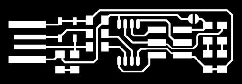
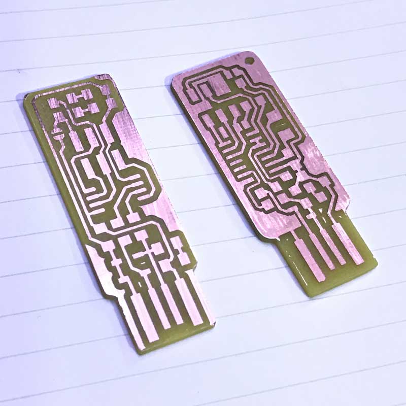
The PCB is composed of a thin layer of copper, measuring in just microns of thickness, laminated onto FR1, phenolic paper. The pattern of copper connects a series of electronic components with electricity. If any unintentional connections are made, the whole system may be fried. While in subsequent posts, I will explore designing the etching patterns, this time around, I am using an open-source project developed in the FabLab ecosystem: the FabTinyISP version of an AVR ISP programmer/board. You can download the same PNG files I used for the traces and the board outline and read detailed build instruction on the FabTinyISP page or directly:
♻ FabTinyStar - Traces (1000 dpi) ♻
♻ FabTinyStar - Outline cutout (1000 dpi) ♻
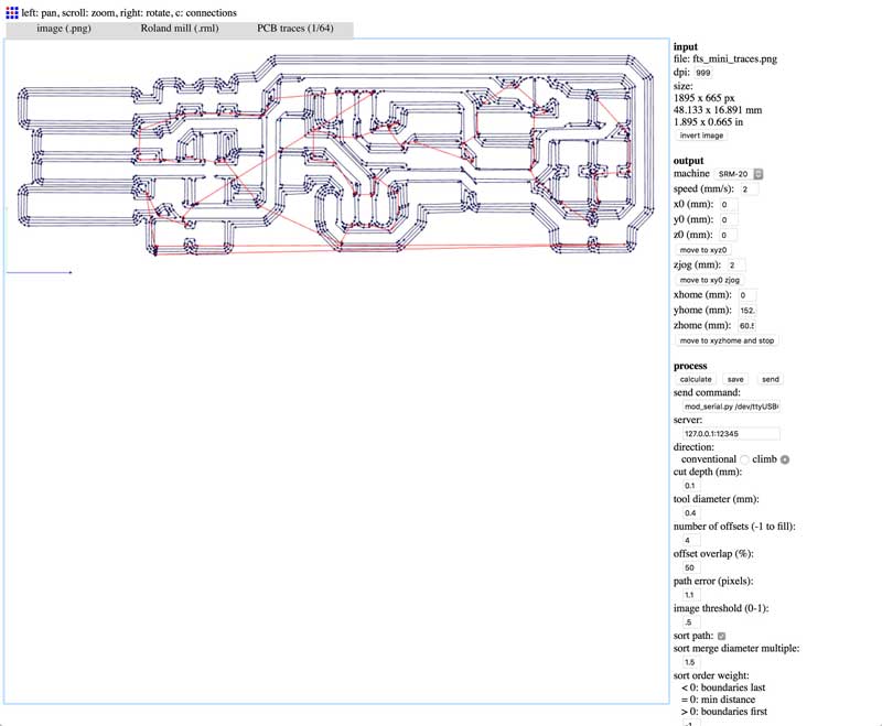
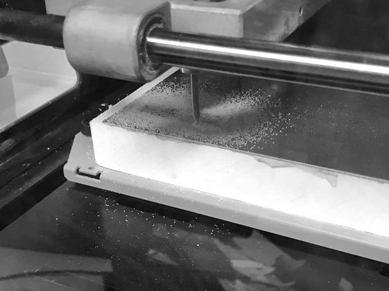
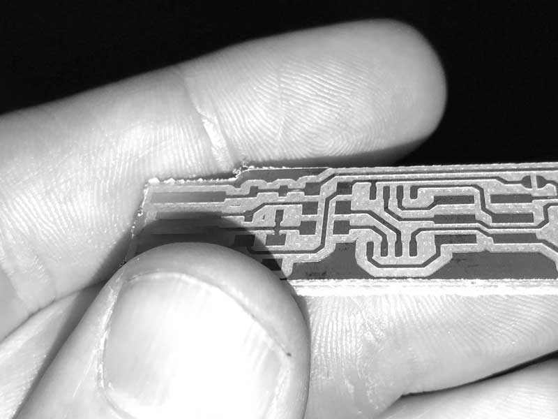
The first image is the traces. The white area will be copper conductive tracks, pads and an USB connector on the left. I will direct the mill to cut away copper around these zones, starting on the edge of the white and working outward. The second, the outline, will be a rough cut through the copper lamination and FR1 substrate. For the outline, the mill will cut a series of overlapping, successively deeper cuts until it clears the substrate.

The image files need to be converted into instructions for the CNC table top mill. This is delivered in the language of paths. Using Fab Modules, you can upload an PNG file (and many other file types), dictate Roland mill, choose the machine type (in FabLabO's case, SRM-20) and the module will output a file for the mill. Fab Modules produce files for different processes using machines typically found in Fab Labs. Setting for milling the traces, use a slower speed: 2mm/s. The outline can be faster: 3-4mm/s. Also set the zjog, the distance the mill head moves above the milling surface between paths (represented by red lines in the image below). A lower zjog will result in a quicker job. Too low, and the endmill may scratch the surface between paths, especially if the surface happens to be warped. More on that later. I set the zjog to 2mm. For the traces, the cut depth only needs to slice through the copper, which is measured in microns of thickness. The tool diameter is based on the end mill that will be used. If there are problems with paths not flowing through certain zones of the PNG, it may be due to that zone measuring inside the diameter of the end mill. The number of offsets, or number of paths the mill cuts emanating from the white zones, is a variable dependent on what is required of the PCB design. For instance, in this design, after cutting, a small bit of copper will remain to the left of the center two USB connectors if only cutting three offsets. That copper will need to be simply removed by a knife and saves time milling. Overlap is the percentage of the end mill that will cut over an existing cut path. Other settings are automatic or set locally on the machine.
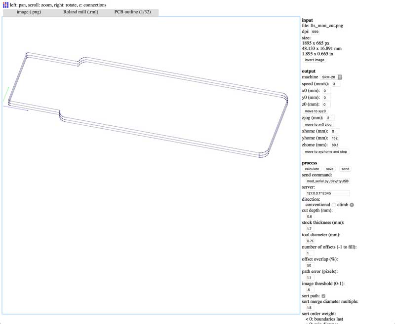
Some slight differences need to be accounted when cutting the outline. First, the cut depth defines the step down of each cut. Second, stock thickness is the thickness of the material plus a little extra to ensure the cut goes all the way through. In the image, the paths are stacked vertically representing successively deeper cuts. The mill is unable to cut through the entire depth of material in one sweep.
To preserve the end mills, it is critical to ensure the material is not warped whatsoever. Apply double sided tape across the entire back surface and adhere the FR1 (copper side up) onto the milling substrate, a chunk of high density foam.
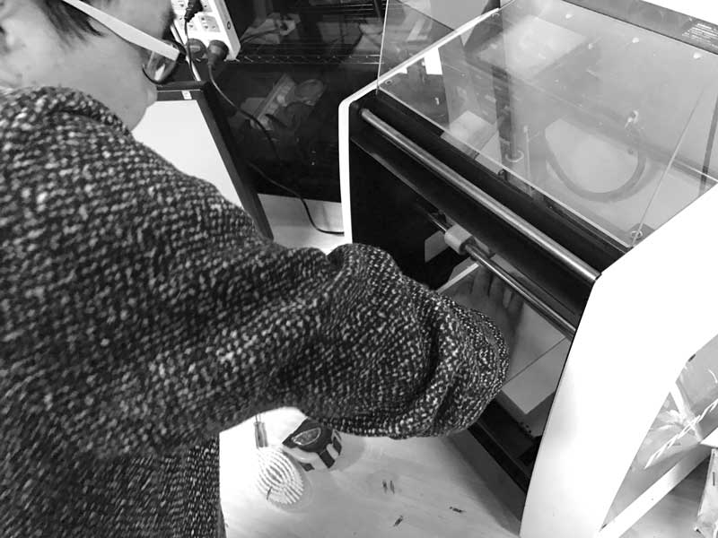
The output files need to be uploaded to the mill via a simple application, here: VPanel of SRM-20. The traces are milled first. This uses a 1/64" endmill which is carefully loaded into the mill head. Before starting the job, set the XY and Z origins by manually maneuvering the end mill to the desired lower-left corner of the job. Then slowly lower the endmill near the surface, check that the XY coordinates are as tight to the area of unused material as possible then set XY origin. Finally, manually reset the height of the bit (loosen, gently drop down, tighten while holding the endmill to ensure it does not move upwards). Set the Z origin before moving the bit up a few millimeters. Now the mill is prepared for cutting.
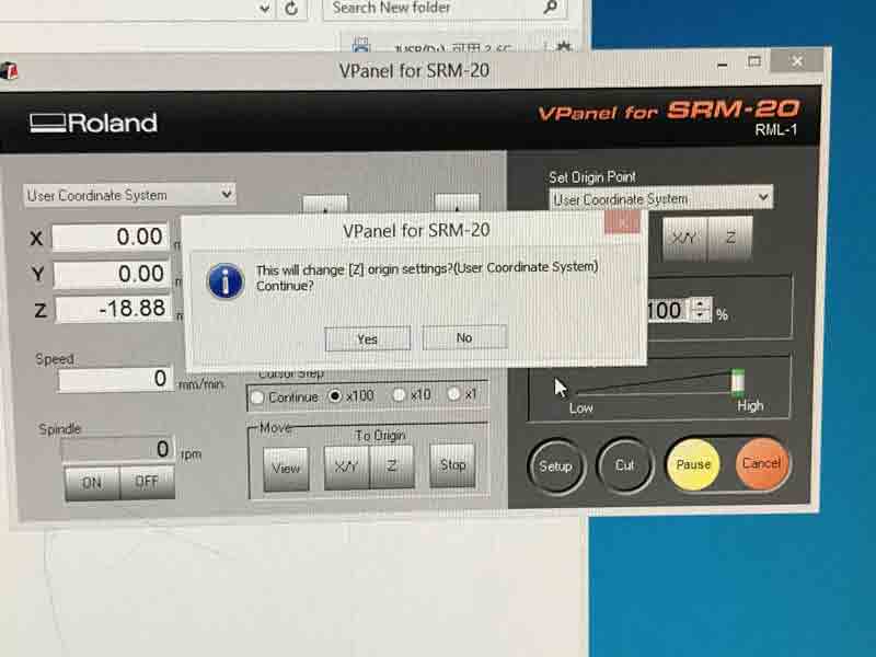
Mill the traces. Thoroughly clean the excess debris in and around the mill with a shopvac or similar. A well-maintained mill is an operational mill. Then change the end mill for the outline, in this case 1/32". Reset the Z origin in the same manner as before. Cut.
Sometimes many files are forgotten on an OS's desktop with nearly identical names for similar jobs. I milled a similar ICSP. Not the one I wanted. I planned to move forward with it regardless but I was talked out of it by fellows in the lab for fear the soldering would be too difficult for a first timer and the microcontroller this board was designed for was not as capable.
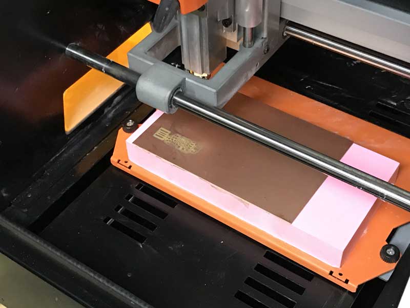
The PCB is cut. Deburr the board: Scrape the copper until it is shiny with a straight edge, like a utility blade, and clean of debris from milling. Then wash it with soap and water. Oils from our hands may slowly etch the copper over months. A working ICSP might become faulty.
I will post links to resources I have found helpful here.
Share this post...
« Previous post :: Wild Cardboard : Fabbing, Branching, Versioning
Now the real adventure begins. In a perfect world this would fit together on the first cut. I am going to assume it is not a perfect world and rely on the flexibility of my parametric model to adjust to the imperfections. The first big challenge will probably be successfully bending, or maybe not. I do not have prior experience with kerf pattern flexure joints. If I clear the bending hurdle, the center joints along the ribbons will probably be tricky because I am having to make an assumption on how this will behave prior to building the model. Testing...
Next post :: Arduino IDE, introduction »
This is Arduino: a family of open-source, programmable Atmel microcontroller-based boards an abstraction on top of standard C syntax and libs a cross-platform IDE a bootloader that can upload code without a hardware programmer a micro-USB port to plug into the computer, digital/analog input/output pins, a separate power jack, an ISP header, and a reset button For my purposes today, I will be using the Arduino IDE, an application written in Java in combination with my own fabbed TinyISP. In my limited experience, it is quite similar to Processing. (Unfortunately, I have forgotten everything else about Processing.) Programs may be...